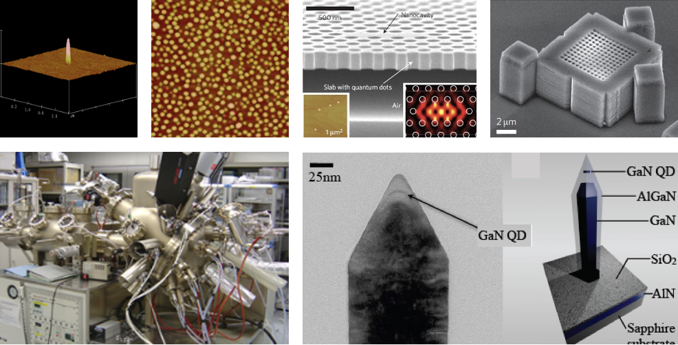
Quantum nanostructure fabrication
Quantum nanostructures such as quantum dots and nanowires that emit light in a wide range of wavelengths from deep UV to mid-IR wavelengths have been realized by molecular beam epitaxy and metalic organic chemical vapor deposition. In addition, new types of lasers and platforms of cavity quantum electrodynamics have been demonstrated by embedding quantum dots in optical nanocavties such as two-dimensional photonic crystals, three-dimensional photonic crystals fabricated, and nanowires.
The main materials and nano-quantum structures that have been developed are as follows.
- Gallium nitride quantum dots and nanowires
- Gallium arsenide quantum dots/nanowires (on GaAs/InP/Si substrates)
- Nanobeams, 2D slabs, and 3D photonic crystals embedded with gallium arsenide quantum
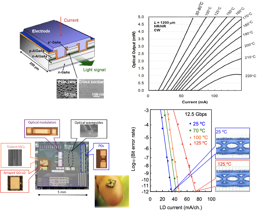
Quantum dot lasers for photonic-electronic convergences (silicon photonics)
The concept of quantum dots for laser application was proposed by Y. Arakawa and H. Sakaki in 1982. In collaboration with QD Laser Inc., we have developed a quantum laser with the world’s highest operating temperature (220°C) and realized novel lasers such as nanowire quantum dot lasers, three-dimensional photonic crystal quantum dot lasers, and topological quantum dot lasers. In the FIRST and NEDO projects, we first fabricated silicon optical integrated circuits with quantum dot lasers and demonstrated the impact of quantum dot lasers in silicon photonics (Photonic and electronic convergence). This achievement was led to the optical I/O core chip developed by AIO Core Inc.. In addition, silicon hybrid quantum dot lasers were fabricated using MBE direct epitaxial growth on (100) just substrate and wafer bonding techniques.
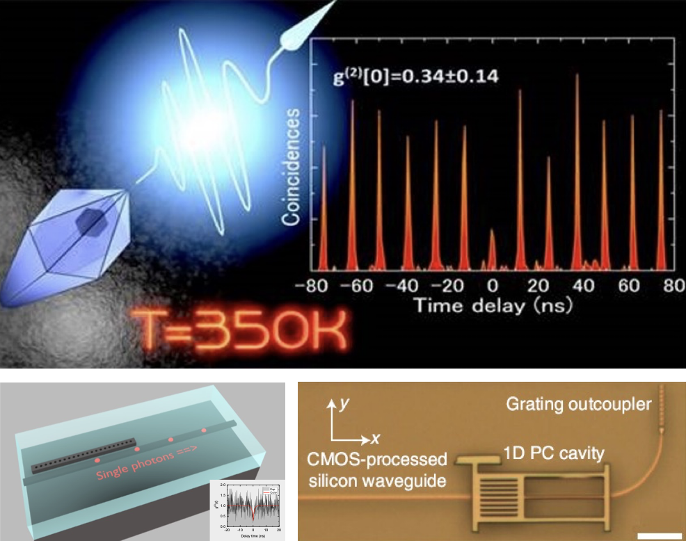
Nano quantum photonics
We have contributed to the development of quantum photonics based on quantum dot technology. Using a telecommunications wavelength band InAs/InP quantum dot single-photon source developed jointly with Fujitsu Laboratories, a quantum key distribution experiment was demonstrated over 120 km (the longest distance in the world in 2012) in collaboration with NEC. In pursuit of a semiconductor single-photon source that can operate at room temperature, we achieved the world’s highest temperature of 350 K for a semiconductor single-photon source via GaN nanowire quantum dots. Furthermore, we realized an InAs/GaAs single-photon source coupled to a silicon waveguide on an SOI substrate using a transfer printing method.
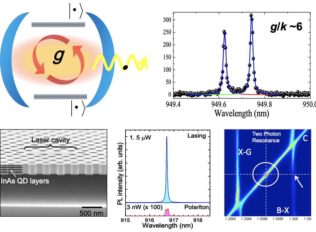
Quantum dot cavity-QED
In 1992, we first observed the strong coupling (Rabi splitting) in solids in a semiconductor vertical microcavity. This achievement is positioned as the starting point of today’s semiconductor cavity quantum electrodynamics. In quantum dot and photonic crystal nanocavity coupled systems, we obtained the highest value of vacuum Rabi splitting for quantum dot systems. A single quantum dot laser that is the ultimate laser, as well as a highly-efficient two-photon emitting device, based on the strong coupling regime was also demonstrated, breaking new ground in solid-state quantum electromagnetic mechanics.